Fabrication Tools
We have no of Equpiment in the class 10000 class clean rooms to provide Fabrication Tools
DILASE 250
- Make (Manufacturer): KLOE
- Light source used: Laser (laser diode)
- Travel Range (Used): 100mm X 100mm
- Materials used: Kloe photoresist (K-CL, K-NG), Positive photoresist
- Wavelength: 375nm
- Writing speed: up to 100m/s
- Laser beam width: from 1um to 50um
- Objective: 10X
- Limitation: cannot go below 1um.
- Company URL:KLOE, France
- Operator: Ms Sayma Ayaz
- Contact: 0512 259 6264
- E-mail: [email protected]


Maskless Photolithography SF 100
- This is mask less photolithography machine by using mask less technique we can directly transfer digital mask onto the substrate without using any physical mask.
- Make (Manufacturer): Micro Intelligence Patterning
- Types of sample to be analyse: Thin film only
- Wavelength Used: 365nm, 405nm and 436 nm. Selectively
- Power Source: UV
- Optics: Reduction and non-Reduction
- Limitations: Cannot go below 5um, used only glass and silicon wafer substrates, high resolution, area cannot go above 11mmX8mm.
- Company URL:IMP, LLC
- Operator: Ms Sayma Ayaz
- Contact: 0512 259 6264
- E-mail: [email protected]


Maskless Photolithography SF 100
- This is also mask less machine, digital mask is used. This is a modified version of SF100. We have some more modes in it.
- Make (Manufacturer): Micro Intelligence Patterning
- Types of sample to be analyse: Thin film only
- Wavelength Used: 365nm, 405nm and 436 nm. Selectively
- Power Source: UV
- Optics: Reduction and non-Reduction
- Limitations: Cannot go below 5um, used only glass and silicon wafer substrates, high resolution, area cannot go above 11mmX8mm.
- Company URL:IMP, LLC
- Operator: Ms Sayma Ayaz
- Contact: 0512 259 6264
- E-mail: [email protected]


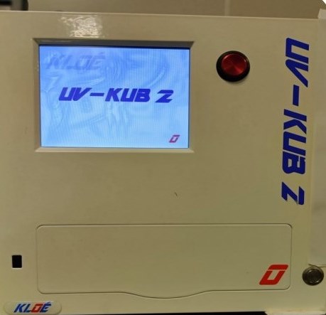
UV- KUB
- Make: KLOE
- Model: UV-KUB 2
- EMISSION SPECTRUM:365nm UV
- Function: Enables to reach resolutions down to 1µm with a physical mask.
- Range: 4 inch wafer
- Types of material analysed: Thin films
- Types of samples analysed: Glass , silicon
- Company URL: UV-KUB 2
- Operator: Ms Sayma Ayaz
- Contact: 0512 259 6264
- E-mail: [email protected]
- Description: This is a mask aligner, in this system we need a physical mask for fabrication.


Molecular Printer
- Make: Synth Nano
- Capacity: 250ml * 2
- Light source used:Mercury arc lamp
- Operator:
- Contact: 0512 259 6264
- E-mail:


- The UV-KUB 2 is a compact exposure-masking system equipped with a LED based optical head, collimated and homogeneous. Its masking function enables to reach resolutions down to 1µm. This system is compatible with any of the most popular photoresists such as AZ series, Shipley series, SU-8 and K-CL series.
- Objective: 4X, 10X,20X
- Limitation: Cannot go below 1um, used only glass and silicon wafer substrates.
- Highlights: Low resolution, we can expose large area, we can do stitching.
Harrick Plasma
- Approved Abbreviation:Plasma cleaner
- Make: Harrick plasma
- Model: PLASMAFLO GAS MIXER
- Company URL: Harrick Plasma
- Range: (115V) - (230V)
- Modes: Nitrogen and Argon gas
- Types of material analysed: Glass and Silicon substrates, Polymer fibers and Fibrous scaffolds, Metal films, and Porous membranes.
- Objective:Nanoscale surface cleaning and surface activation
- Highlights:Remove nanoscale organic contamination Enhance adhesion to other surfaces
- Operator:
- Contact: 0512 259 6264
- E-mail: [email protected]


- 6” Dia. x 6.5” L Chamber 30 W Maximum RF Power 37 Lbs., 11” H x 18” W x 9” D
- Objective:Nanoscale surface cleaning and surface activation
- Highlights:Remove nanoscale organic contamination Enhance adhesion to other surfaces
UV-Ozone
- Approved Abbreviation:UV Ozone Cleaner – ProCleaner™ Plus
- Make: BioForce Nanosciences
- Model: UV Ozone Cleaner – ProCleaner™ Plus
- Company URL: UV-Ozone
- Function: It removes molecular levels of contamination to ensure the cleanest possible AFM probes and surfaces.
- Types of material analysed: Glass and silicon substrates, polymer, thin film
- Highlights:It removes molecular levels of contamination to ensure the cleanest possible AFM probes and surfaces.
- Operator: Sayma Ayaz
- Contact: 0512 259 6264
- E-mail: [email protected]


- Voltage: 110V, 220V
- Max sample height:25mm
- UV ozone coverage area:4” x 5” (100mm x 125mm)
Solution spin, Flow Coating and Electrospinning
- Make: IMP
- Model: SF100
- Light source used: Mercury arc lamp
- Material used:
- From Positive photoresist max 3um film thickness can be achieve.
- From Negative photoresist max 80 um thickness can be achieve.
- Operator: Ms Sayma Ayaz
- Contact: 0512 259 6264
- E-mail: [email protected]


- Wavelength: 365nm, 405nm and 436nm selectively.
- Objective: 4X, 10X,20X
- Limitation: Cannot go below 1um, used only glass and silicon wafer substrates.
- Highlights: Low resolution, we can expose large area, we can do stitching.
FESEM coupled with Electron Beam Lithography
- Make: IMP
- Model: SF100
- Light source used: Mercury arc lamp
- Material used:
- From Positive photoresist max 3um film thickness can be achieve.
- From Negative photoresist max 80 um thickness can be achieve.
- Operator: Ms Sayma Ayaz
- Contact: 0512 259 6264
- E-mail: [email protected]


- Wavelength: 365nm, 405nm and 436nm selectively.
- Objective: 4X, 10X,20X
- Limitation: Cannot go below 1um, used only glass and silicon wafer substrates.
- Highlights: Low resolution, we can expose large area, we can do stitching.
Reactive Ion Etching
It can handle wafers up to the size of 100mm (or 4 inches) in diameter. The system can be used for etching of oxides, nitrides, polymers, silicon. The system can accommodate a wide range of process gases.- Make: Planar tech
- Model: Planner RIE - 4C System
- Range: Oxygen, Nitrogen & SF6.
- Types of material analysed:: Glass, Silicon, Thin films, Polymers
- Highlights: Plasma etching.
- Company URL: Planner Tech
- Operator: Ms Sayma Ayaz
- Contact: 0512 259 6264
- E-mail: [email protected]


